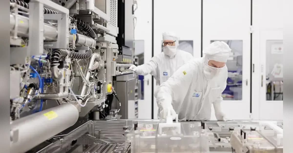
Major semiconductor manufacturers are adopting ASML chipmaking machines to expand production capacity across global facilities. Samsung Electronics and Taiwan Semiconductor Manufacturing Co. confirmed initiatives to integrate high-numerical-aperture extreme ultraviolet systems in coming years. Both firms also joined Intel in adopting larger 12-inch photomasks, according to Ars Technica.
Shift to Larger Photomask Standards
The move from traditional 6-inch photomasks to 12-inch designs marks a significant operational adjustment for the industry. Photomasks function as stencils that transfer circuitry layouts onto silicon wafers during manufacturing. ASML Chief Technology Officer Marco Pieters stated to Bloomberg that switching to larger stencils could lift output productivity by up to 40 percent on advanced production lines.
Memory supplier SK Hynix is evaluating participation in the industry consortium managing the photomask standard update. Standardizing bigger templates allows chipmakers to print larger patterns in single exposures, decreasing processing time for complex processors used in computers and consumer hardware.
Adoption Timelines for ASML Chipmaking Machines
Fabricators have set clear roadmaps for incorporating high-numerical-aperture ASML chipmaking machines into upcoming fabrication lines. Samsung expects to deploy the lithography equipment for memory production by 2028. TSMC plans to introduce the hardware around 2030 to manufacture chips for corporate clients including AMD, Apple, NVIDIA, and Qualcomm.
Intel began integrating the equipment earlier, applying it to high-volume manufacturing of its Panther Lake mobile processors in July 2026. Each high-NA system costs approximately $400 million and uses specialized optical components from Zeiss Group to project light patterns with extreme precision.
Production Demands and Market Pressures
Expanding manufacturing capacity remains a core priority as demand surges for artificial intelligence infrastructure. The construction of massive data centers has tightened the supply of specialized memory components, causing price pressure across mobile devices, laptops, and gaming hardware. Deploying advanced ASML chipmaking machines will help lower per-unit wafer costs as production volumes grow.
International Competition and Export Controls
Access to advanced lithography remains subject to tight regulatory limits. Trade controls by Dutch and American authorities prevent ASML from shipping high-end EUV equipment to Chinese manufacturers like SMIC. Industry analysts note that developing domestic alternatives remains difficult, with component suppliers estimating that rival systems could take more than a decade to replicate independently.